Silicon photonics
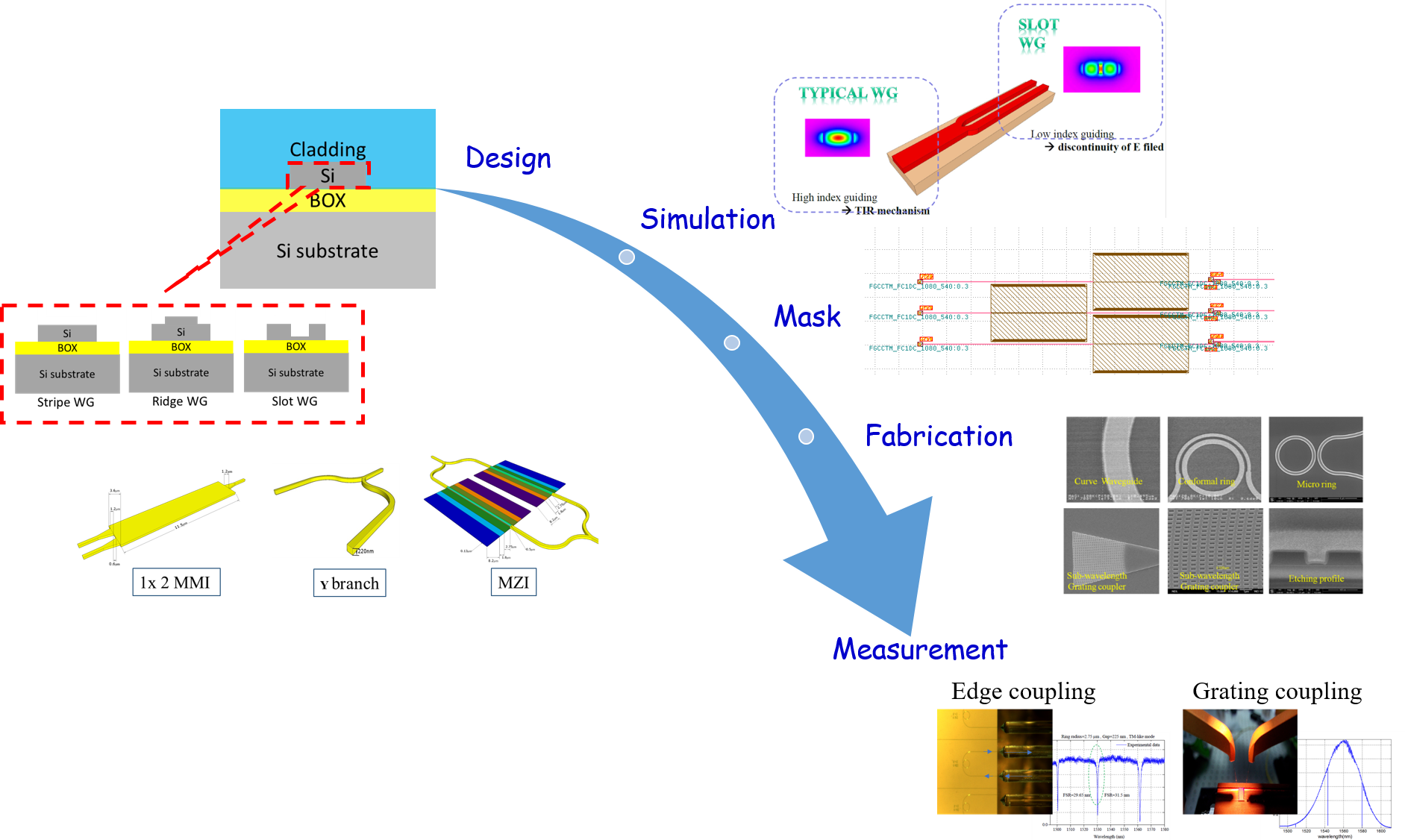
Silicon photonics has emerged as a mature technology for photonic integrated circuits (PICs), owing to its inherent high-bandwidth capabilities for long-distance transmission and seamless compatibility with silicon CMOS process technology. This technology has paved the way for numerous applications, including data centers, high-speed computing, and advanced sensing technologies. Our research focuses on the design and development of a wide range of silicon photonics waveguide devices tailored for diverse photonic applications."
The design flowchart of Si/ SiN WG
Over the past few years, we have developed a design process for silicon photonic devices, including the selection of core and cladding materials, structural design, simulation, layout creation, fabrication, and performance measurement. To date, we have successfully realized a variety of passive waveguide devices and integrated them into applications across diverse fields.
The fabrication process of SiN WG (in TSRI)
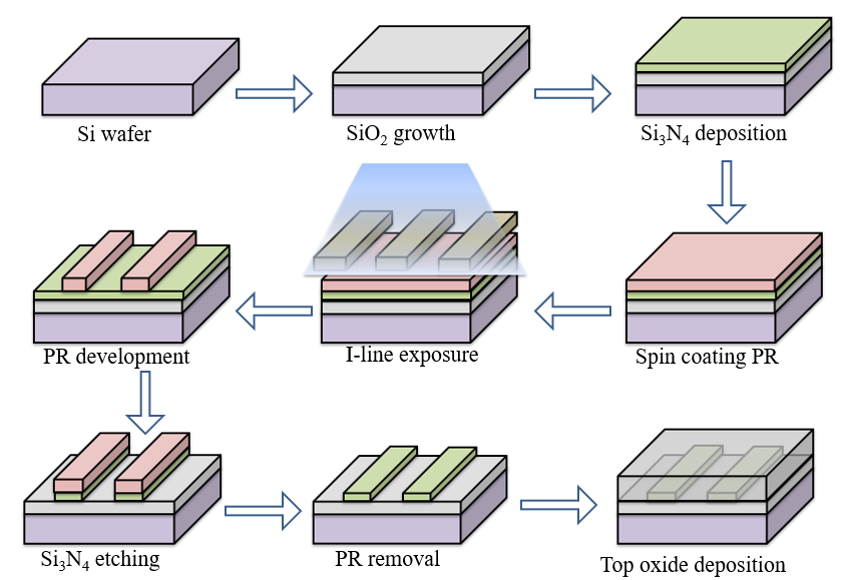
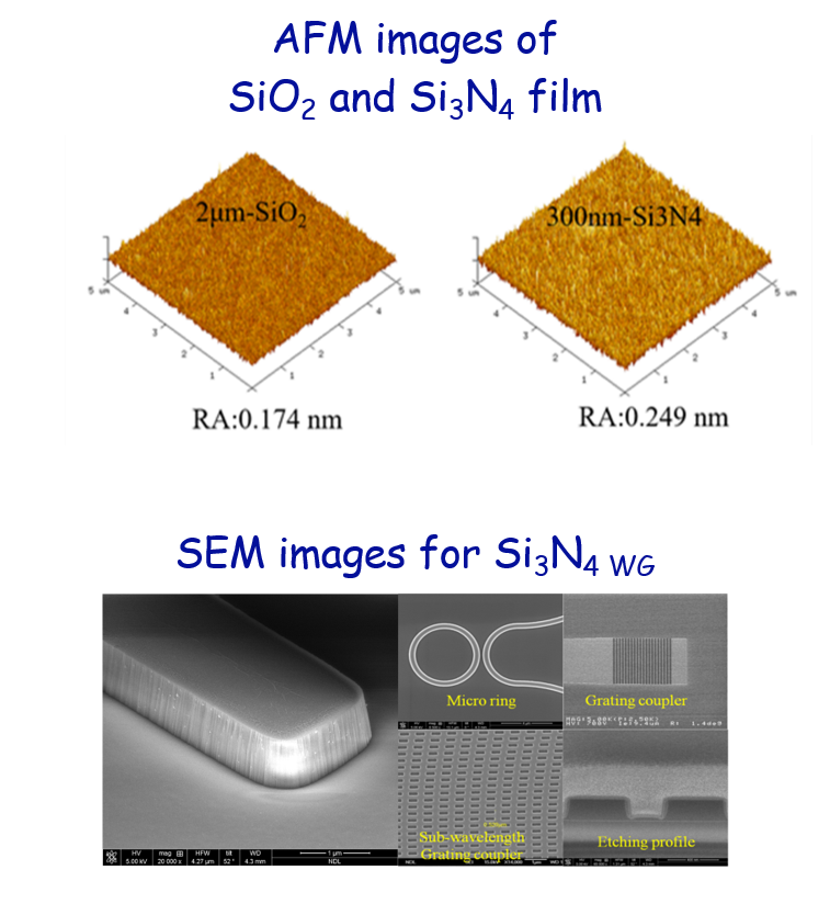
To fabricate silicon photonic devices, we collaborated with the Taiwan Semiconductor Research Institute (TSRI) to develop a waveguide platform utilizing their complete CMOS fabrication facilities. Our focus is on silicon nitride (Si₃N₄) as the core material, owing to its numerous advantages, including high fabrication tolerance, low optical loss, and a wide spectral range. To date, we have achieved the fabrication of Si₃N₄ waveguides with low optical loss of approximately 2–3 dB/cm and have developed various innovative waveguide structures.
Measurement system for WG
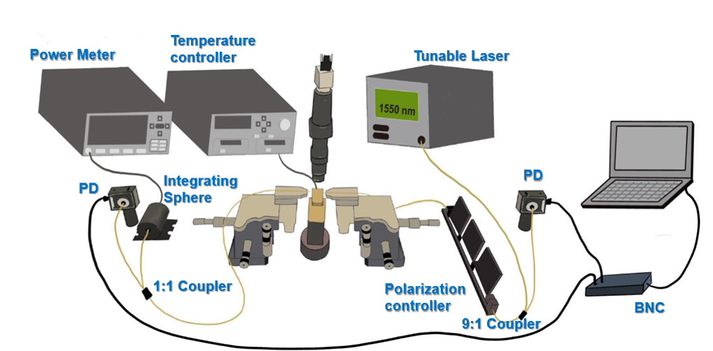
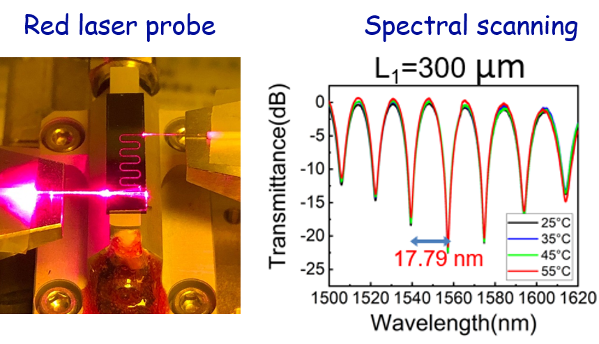
We have established an edge coupling measurement system to evaluate the performance of our designed waveguide devices. The system features tunable laser light sources in the NIR region, precise motorized stages, various optical components, and detectors. Recently, we upgraded our setup to include a grating coupling measurement system for enhanced versatility and functionality.
Passive Si/ SiN/SU8 WG
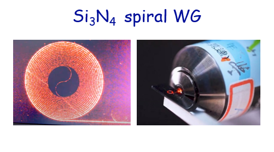
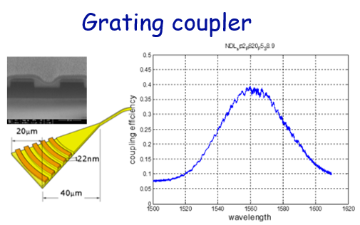
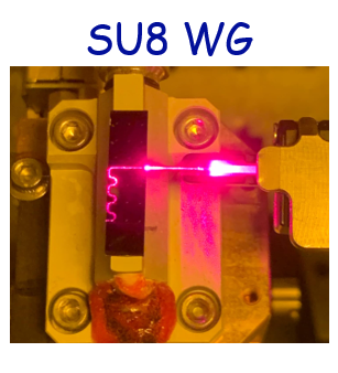
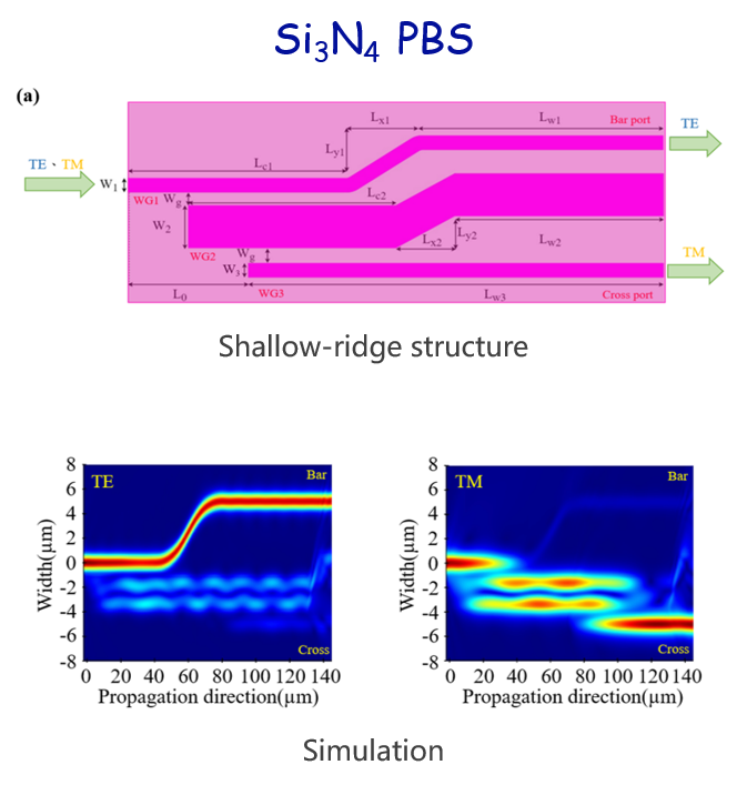
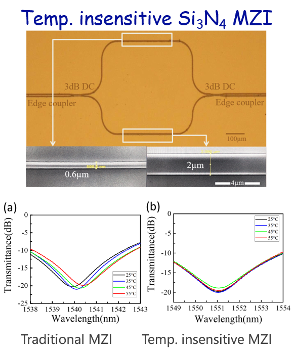
Over the past few years, we have successfully designed and fabricated several common passive waveguide devices, including channel waveguides, grating couplers, polarizing beam splitters (PBSs), microrings, directional couplers, and Mach-Zehnder interferometers (MZIs). Additionally, we have initiated the fabrication of SU-8 waveguides to enable cost-effective applications.
Chinese Journal of Physics 92, 1078–1084 (2024).
Silicon photonic WG with LC claddings

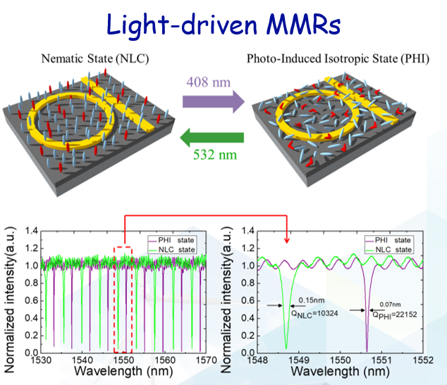
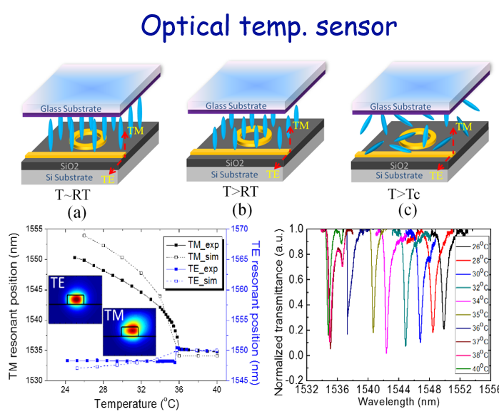
Due to inherent material limitations and weak electro-optical effects, silicon and silicon nitride alone cannot fulfill all-optical functionalities. To address this challenge and meet the demands of diverse silicon photonic integrated chips, we have incorporated liquid crystals (LCs) as a cladding material, enabling enhanced tunability and expanded functionalities.
- Opt. Exp. 21, 10989-10994 (2013).
- Opt. Exp. 22, 17776-17781 (2014).
- Opt. Exp. 24, 1002-1007 (2016).
- Opt. Exp. 24, 22892 (2016).
- Opt. Express 28, 29345-29356. (2020).
- IEEE Photon. Technol. Lett., 33, 796–799, (2021).
- Opt. Lett. 47, 3940-3943 (2022).

